
What Are Biodegradable PCBs and Why Do They Matter?
- Key Takeaways
- What are Biodegradable PCBs?
- How are Biodegradable PCBs Made?
- Environmental Impact of Biodegradable PCBs
- Benefits of Biodegradable PCBs
- Challenges in Biodegradable PCB Technology
- Applications of Biodegradable PCBs
- Current Research and Advancements
- Future Prospects for Biodegradable PCBs
- Conclusion
- Frequently Asked Questions
Key Takeaways
- Biodegradable PCBs (Printed Circuit Boards) to address e-waste They’re made with materials that break down naturally, offering an environmentally conscious alternative to conventional PCBs.
- Biodegradable PCBs are composed of natural fibre substrates, organic substrates, and water-soluble polymers. These materials are a more sustainable alternative to typical non-degradable materials, which makes them a green solution.
- These PCBs greatly minimize the environmental impact by decreasing the long-term build-up of non-biodegradable waste and encouraging more sustainable disposal methods.
- When compared to conventional PCBs, biodegradable PCBs have a vastly lower carbon footprint. They save precious resources and are well-suited for low-cost, short-lived or disposable electronic devices.
- The main obstacles today are lack of durability and increased expense. We clearly need more research to improve performance and scalability for mass adoption.
- As you can see, researchers are creating exciting advancements in biodegradable PCB technology. This innovation holds great promise across various sectors, including healthcare, consumer electronics, and environmental monitoring.
Biodegradable PCBs are revolutionizing our approach to electronic waste. These biodegradable PCBs, engineered to degrade, use eco-friendly materials that minimize environmental impact by allowing the boards to break down naturally.
While traditional PCBs are made with non-degradable materials, biodegradable PCBs incorporate plant materials such as natural fibres and biopolymers. By reducing what is sent to landfills and reducing the impact of hazardous components, this innovation furthers sustainable manufacturing and waste management.
Our researchers and engineers are working hard to continue improving durability and performance. Their mission is to produce the most technologically advanced electronics possible, while being environmentally friendly.
Industries are welcoming greener alternatives in record numbers. Biodegradable PCBs represent a practical step towards reducing waste and promoting a circular economy in the world of technology. They signal a breakthrough toward more sustainable electronics.
What are Biodegradable PCBs?
Biodegradable printed circuit boards (PCBs) represent a significant advancement in addressing the growing issue of e-waste. This ground-breaking material is designed to minimize the environmental impact created by e-waste. E-waste is a huge environmental hazard today, as the components of e-waste do not decompose.
Biodegradable PCBs offer a more promising solution, possibly reducing this waste by a remarkable 60%. These boards are made from bio degradable polymers, materials that science has shown to be non-toxic and biodegradable. Unlike traditional PCBs, typically composed of plastics and metals, biodegradable PCBs are created to break down organically, reducing ecological harm.
The ingredients that go into biodegradable PCBs are all-natural materials – like jute, flax, silk, cellulose and even wood. These materials are helping advance sustainability, while providing the mechanical strength that matters. Plus, they provide the electrical conductivity required for many of today’s electronic devices.
Production techniques such as 3D printing or inkjet printing allow for production in a distributed and efficient manner. They provide extreme precision in the manufacturing process. This adaptability makes sure they remain able to satisfy the needs of a rapidly evolving electronic application landscape.

At the end of their life cycle, you can compost biodegradable PCBs rather than throwing them in landfills. This practice intentionally bolsters ongoing waste management activities. Given their ability to fully replace conventional PCBs, they represent an exciting innovation in the world of sustainable technology.
How are Biodegradable PCBs Made?
Biodegradable PCBs, or biodegradable printed circuit boards, are created with the latest materials and technology. These innovations are designed to help them minimize their environmental footprint drastically. A solid-state electrolyte is a key enabler in these designs.
It partners choline-based ionic liquid with polysaccharide to increase efficiency and performance. This specific composition creates an optimal performance standard while allowing the board to be more environmentally friendly and break down in nature. Novel plant-based materials like silk fibroin, cellulose, and gelatine provide excellent biodegradability.
This contributes to the fact that these PCBs are not only environmentally friendly but are extremely efficient. These bio-based materials provide a feasible alternative to produce completely biodegradable PCBs with hardly any performance hits at all.
The production process usually includes additive manufacturing, a process in which biodegradable materials are added in layers to create the PCB. This technique provides good control over the structure to tune it to achieve the best possible mechanical properties.
For instance, polylactic acid (PLA) is commonly used because it’s strong, flexible, and biodegradable. Mixing biodegradable materials with conventional PCB manufacturing processes makes for some very interesting boards. These boards are biodegradable, recyclable and reusable!
This revolutionary approach could ultimately lead to a 60% reduction in electronic waste. Moving from conventional PCBs to biodegradable PCBs is a big move for sustainable electronics, especially in this age of increasing e-waste pollution.
Environmental Impact of Biodegradable PCBs
The move to biodegradable PCBs represents a real improvement in environmental impact at both the production and disposal stage. Traditional PCBs contribute heavily to e-waste, with millions of metric tonnes generated annually. This waste problem is growing exponentially.
So far, just 11% is recycled sustainably, which manages to offset 15 million tonnes of CO2, but there’s a long way still to go. Fortunately, biodegradable alternatives offer a realistic answer to this dilemma. For example, replacing copper etching production methods with silver ink printing on FR4 substrates reduces carbon emissions by around 80%.
This one change alone represents a carbon saving of 10.5 kilograms per square metre of circuit board made. The environmental impact goes beyond carbon emissions. The “raw material” stage, which includes the production of copper-plated substrates, makes up more than 43% of total carbon emissions associated with PCBs.
Biodegradable PCBs address this concern by using biodegradable materials like pure PVA films. These films show a Young’s modulus of 2.32 ± 0.3 GPa and a tensile strength of 25.3 ± 3 MPa, ensuring their robustness.
In addition, these substrates resist high temperatures in excess of 200°C, making them suitable for compatibility with conventional reflow processes. This structural dependability makes it easier to integrate into current manufacturing ecosystems, but most importantly it minimises the impact on the environment.
All in all, the assembly of such PCBs shows an overall 10% reduction in environmental load versus traditional assembly methods.
Benefits of Biodegradable PCBs
Safer, biodegradable PCBs are an effective and much-needed solution to the rising tide of e-waste. Currently only £8.2 billion worth of e-waste is recycled and sustainably recovered each year. This is a surprisingly large opportunity — it could cancel out the equivalent of 15 million tonnes of CO2 emissions and provide significant additional environmental benefits.
Because biodegradable PCBs break down naturally, the amount of waste that goes into landfills is greatly reduced. This innovation addresses a major hurdle in sustainable electronic waste management.
You can also make these PCBs from renewable resources including natural fibres and bioplastics. This methodology makes a huge stride in lowering our reliance on traditional materials that consume non-renewable resources.
Sustainable manufacturing processes such as 3D printing and injection moulding have a considerably lower energy footprint. These approaches provide an important co-benefit of reducing greenhouse gas emissions. This makes the whole production and disposal lifecycle of biodegradable PCBs inherently more environmentally friendly.
Biodegradable PCBs can be modified to meet specific requirements for innovative applications. Their flexibility makes them a good fit for wearable electronics such as smart clothing and fitness trackers.
Medical devices – especially implantable ones like pacemakers and neurostimulators – benefit from their biocompatibility with the human body. They’re designed for recyclability and reuse.
This method supports all aspects of a circular economy and dramatically decreases the amount of waste produced by our electronics.
Challenges in Biodegradable PCB Technology
The path to creating biodegradable circuit boards has not been an easy one. It starts with the requirement to tailor PCB substrate characteristics, manufacturing processes, and end-use applications. It’s a matter of finding the right sustainable materials that are environmentally conscious but meet the needs of the technology.
Others, such as cellulose and silk fibroin, offer exciting possibilities. While they have potential, they’re frequently lacking in terms of robustness and flexibility, qualities that are often necessary for some electronics.
One significant hurdle has been conductivity. This is because biodegradable PCBs typically have less conductivity than traditional PCB materials, restricting their utility in high-demand applications. As a result, there is a critical challenge for engineers to improve conductivity while maintaining biodegradability.
The degradation process is unpredictable. Humidity, temperature, and exposure to other elements all factor heavily into how and when PCBs degrade. This variability can lead to unreliable performance and even obsolescence.
Cost is yet another major hurdle. With manufacturing techniques still in their infancy, the fabrication of biodegradable PCBs is pricier than their conventional counterparts. The most important challenge, though, is scaling up production capacity to meet industrial demands for recyclable PCB substrates.
Existing processes find it difficult to pivot to high-throughput, large-scale manufacturing. Further, integrating these boards with other electronic components increases the complexity due to their distinct physical and chemical characteristics.
Environmental impact studies, while continuing, are not definitive. A much clearer picture is needed to determine the net benefits. Creating biodegradable alternatives to PCBs requires expertise from materials science, electronics engineering, and environmental science, highlighting the multidisciplinary work involved.
Applications of Biodegradable PCBs
Biodegradable PCBs (printed circuit boards) are changing the way we think about electronics by providing a sustainable solution to traditional PCB materials. They have numerous applications in agriculture, electronics, and defence industries, alleviating environmental damage while maintaining the necessary performance.
One major frontier is consumer electronics. Devices such as mobile phones, tablets, and wearable technologies are designed with short lifespans as a result of fast-paced technological improvements. With biodegradable PCBs, these devices can be disposed of in a much more responsible manner.
Once discarded, these boards break down naturally, helping to lessen our growing pile of electronic waste. For example, a biodegradable PCB material used in a fitness tracker can decompose under industrial composting conditions within months, providing a viable option for disposing of outdated tech.
Another very exciting application is in the medical device space. Biodegradable PCBs open the door for new temporary implants, like advanced sensors that monitor healing processes or deliver medication. Unlike traditional PCBs that require surgical removal, these boards ultimately dissolve safely in the body, removing the need for invasive removal procedures.
As a result, it decreases risks to patients and the complexity of medical procedures. For instance, a biodegradable sensor could track a patient’s recovery from surgery and harmlessly dissolve once its work is done.
Expanding the applications of renewable materials is key to achieving the energy transition. Biodegradable PCBs can be utilized in small-scale solar panels or in sensors for wind turbines engineered for temporary installations, ensuring that even renewable technologies are less impactful on the environment.
Current Research and Advancements
With vision inspired by new design paradigms and enabled by cutting-edge material science, the creation of biodegradable circuit boards has advanced rapidly. Through several iterations of PCB designs, researchers have managed to reach a catechol purity of 98%. This high level of purity speaks to the precision involved in the material processing, allowing for superior performance while keeping sustainable qualities intact in the recyclable PCB substrate.
These PCBs are produced with substrates that are dimensionally stable to organic solvents. In water-rich environments, they can completely dissolve in as little as 5 to 15 days. This quick biodegradability is one action towards reducing the amount of electronic waste generated by traditional PCB materials.
Materials developed for use in these PCBs have set new standards for mechanical properties. With 2 wt% DFDP, poly(lactic acid) (PLA) attains a tensile strength of 59.9 MPa, which is among the highest tensile strength values. This formulation increases elongation at break by 15.8% and enhances impact strength by 34.3% compared to regular PLA, showcasing the innovative nature of biodegradable PCB material.
New solutions such as PLA in tetrahydrofuran have been developed to recover 98% of the PLA by evaporation methods. These initiatives help to ensure that no material goes to waste, further supporting the recycling process in the PCB industry.
Other innovations include high-performance sensors, including one flexible sensor that produced a gauge factor of 1296 or higher when subjected to strain. Among bioepoxy materials, GPTE offers impressive thermal stability, making it suitable for long-term uses in advanced electronics technology.
Future Prospects for Biodegradable PCBs
Biodegradable PCBs present exciting new avenues to mitigate the ever-growing ecological risks associated with electronic waste. The most impressive benefit is the clear reduction in waste, which many estimates suggest will result in 60% less waste. The need for biodegradable electronics is accelerating wearable electronics. The market is predicted to reach £25.2 billion by 2020.
As biodegradable PCBs are being adopted more widely, more devices are using them. This simple change can reduce environmental impact upwards of 10% of the complete assembly ecological footprint.
The potential impacts of biodegradable PCBs reach further than just reducing waste. New advancements in materials have made it possible for these biodegradable PCBs to harvest Wi-Fi ambient RF energy. This innovation paves the way towards creating self-powered devices.
The addition of Frequency Selective Surfaces (FSS) dramatically improves performance. At 2.4GHz, it increases the antenna efficiency by 42% and at 5.2GHz the efficiency level increases to 74%. Those kinds of improvements would be game changers for deployment of energy-efficient technologies.
In the world of manufacturing, 3D printing has transformed the way 3D-printed electronics (3D PE) are produced. This development is a big leap in technology. Surface as thin as 10.7–11.2 μm with surface roughness of 0.4–1.1 μm were obtained, indicating very high accuracy.
Potassium niobate-based screen-printable inks enable piezoelectric layers to be processed at only 120 °C.
Revolutionizing Electronics: How Jiva Materials is Reducing E-Waste with Soluboard®
At Jiva Materials, we are transforming the electronics industry with our innovative product, Soluboard®. Recognized as the world’s first fully recyclable and biodegradable printed circuit board (PCB), Soluboard® directly addresses the pressing issue of electronic waste. Unlike traditional PCBs made from non-degradable materials, we have designed Soluboard® using natural fibers and a water-soluble polymer, significantly reducing its environmental footprint. With this unique product, we aim to enable sustainable manufacturing and promote a circular economy by facilitating the recovery and recycling of components and materials.
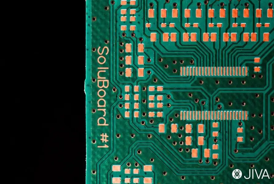
We developed Soluboard® to combat the growing e-waste crisis by providing an eco-conscious alternative that combines advanced materials with practical functionality. While traditional PCBs contribute heavily to global waste due to their complex composition of metals and plastics, Soluboard® dissolves in hot water under controlled conditions. This process efficiently separates electronic components, many of which can be reused, reducing landfill waste and conserving valuable resources.
One of the key benefits of Soluboard® is its seamless compatibility with standard PCB fabrication processes. Manufacturers can easily integrate Soluboard® into their workflows without compromising on quality or performance. Its robust design ensures it meets the demands of modern electronics while offering the added advantage of biodegradability. By using Soluboard®, companies can reduce their carbon emissions by up to 67% compared to traditional PCB materials—helping them meet sustainability goals without sacrificing efficiency or durability.

As the demand for sustainable solutions grows, Soluboard® is already making a significant impact across industries such as consumer electronics, healthcare, and environmental monitoring. At Jiva Materials, we are committed to advancing the capabilities and applications of biodegradable PCBs. By choosing Soluboard®, businesses can play an active role in reducing e-waste and supporting environmentally responsible practices, paving the way for a more sustainable future in technology.
Conclusion
Biodegradable alternatives PCBs offer a new way to think about electronic design. They provide a direct and ubiquitous opportunity to reduce waste and relieve growing pressure on landfills. Composed entirely of natural materials, they biodegrade harmlessly, leaving no toxic residue. All of which leads to a cleaner, more sustainable future for technology.
The benefits are obvious – reduced environmental impact, reduced cost of disposal, and reduced dependence on non-renewable resources. Though challenges like durability and scalability remain, continued research continues to expand what’s possible. Industries from consumer electronics to healthcare to agriculture are already unlocking their potential.
It’s an exciting time to be engaged and help support new innovations in this space. Let’s work together to make greener alternatives the smart, responsible choice. Learn more about this promising new step in the right direction.
Frequently Asked Questions
What are biodegradable PCBs?
Biodegradable PCBs, made from biodegradable materials, are engineered to degrade in the environment, significantly aiding in the recycling process and minimizing e-waste and pollution.
How are biodegradable PCBs made?
They’re manufactured with organic materials, such as cellulose and natural fibres, along with biodegradable pcb materials and bio-polymers, as opposed to conventional metals and plastics, ensuring they can break down without harming the ecosystem.
What are the benefits of biodegradable PCBs?
Biodegradable PCBs, as a new laminate in the PCB industry, will help eliminate electronic waste, cut carbon emissions, and promote the use of sustainable practices while providing equal or better performance compared to traditional PCB materials.
Are biodegradable PCBs environmentally friendly?
Yes. Biodegradable PCBs, made from sustainable materials, are engineered to break down organically, making them a greener alternative to traditional PCB materials and reducing the ecological footprint.
What are the challenges with biodegradable PCBs?
Their main challenges include the lack of durability and high production costs associated with traditional PCB materials, which have not yet achieved the longevity or performance of advanced materials.
Where are biodegradable PCBs used?
Biodegradable PCBs, particularly those made from renewable materials, would find application in disposable electronics, medical devices, and sensors, offering sustainable solutions for short-life devices in the evolving electronics technology landscape.
How does Jiva Materials’ Soluboard® contribute to reducing the environmental impact of traditional PCB manufacturing processes?
Jiva Materials’ Soluboard® is designed to address the significant environmental challenges posed by traditional PCBs. Unlike conventional boards made from non-degradable materials, Soluboard® uses natural fibers and a water-soluble polymer, which allows it to break down naturally. This reduces the buildup of electronic waste in landfills.
Moreover, its unique dissolvable properties enable the recovery of valuable electronic components, minimizing resource wastage. By reducing carbon emissions by up to 67% compared to traditional PCBs, Soluboard® significantly contributes to sustainable manufacturing practices.
What industries are already benefiting from integrating Soluboard® into their electronic manufacturing workflows?
Soluboard® has gained traction in various industries looking for sustainable solutions. Consumer electronics manufacturers are using it to reduce the environmental impact of devices with short life cycles, such as smartphones and wearables. The healthcare sector benefits from Soluboard®’s biocompatible properties in medical devices, including temporary implants and sensors. Additionally, it is being applied in environmental monitoring and renewable energy systems, such as solar panels and wind turbine sensors, further supporting global sustainability efforts
What is the future of biodegradable PCBs?
Innovations in materials, such as biodegradable PCB materials, greater durability, and broader adoption are just a few of the themes. Now researchers are trying to make biodegradable circuit boards more affordable and accessible to different industries.